In this
article:
The Phase Locked Loop
Navigation:
HomeHardware
Software
Techniques
Controllers
Reviews
Index
Introduction
Computers use clocks. Some have both time of day clocks which hold the time and date, but for this article we’re going to focus on the system clocks which are generally fixed frequency square waves that synchronize the operation of various circuits within the computer.
If you have used a microprocessor such as the Arduino, you may have read something like “The system clock is 16 Mhz”. For many programmers, what the actual value is doesn’t matter, as long as it is stated somewhere. But for embedded programmers, knowing what the clock speed is, and how to change it, lets you operate various peripherals.
The system clock, and all of the peripheral clocks it feeds on the STM32F4 series processors, can be rather intimidating at first. But once you get to know it, you may find as I did that it is pretty straight forward.
Clock Sources
Back in the early days of microprocessors, setting up the clock was the job of a separate chip known as the clock controller. This chip would generate a two phase clock and ensure that the timing between power on and the reset line being released to let the CPU run was met. Then in 1976 when the Z80 was introduced it had a built-in clock chip and from that point forward microprocessors generally had a couple of pins dedicated to either a crystal, or a clock input.
The STM32F4 series generally has three possible clock sources.
- HSI - An internal high speed clock based on a trimmed RC network that runs at 16 MHz.
- HSE - An external high speed clock which can either be a crystal or digital clock source like an oscillator.
- MSI - An internal “medium” speed clock based on a trimmed RC network inside the chip.
- LSE - An external low speed clock source which is typically 32.768 kHz which makes generating a time of day clock from it fairly straight forward.
The place where this gets tricky is that the chip also includes an internal phase locked loop (PLL) which can be used to increase the effective clock rate significantly.
Further, one clock feeds many of the peripherals and that can put constraints on the clock speed selected if those peripherals are to work correctly. The most common constraint is that the high speed USB peripheral and Ethernet peripheral require a 48 MHz clock to work correctly.
The Phase Locked Loop
The phase locked loop component inside the chip combines a clock multiplier and one or more clock dividers that feed the clock inputs of the chip. There is a brief description of how phase locked loops work here.
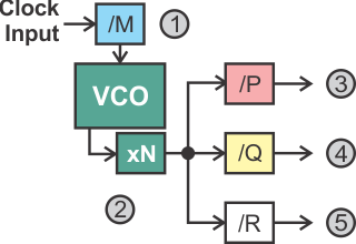
The PLL component is shown above in block form. Different versions of
the chip may have one, two, or as many as four of these on some models.
They all have the same configuration restrictions but they are used for
different parts of the chip, and they all share the same ‘M’ divider. In the
diagram, like in the datasheet, the notation /<letter> means "divide by
value in field <letter>, and the xN notation is “multiply by N.”
So lets take a quick tour of this gizmo starting with step 1. At the top
an input clock signal is fed into the PLL. This clock is either the HSI clock
at 16 MHz or an external clock (set by crystal or oscillator) for most of the
F4 series. Some of the L4 variants have a medium speed internal clock
called MSI and some can use the lowspeed clocks (either LSE or LSI) to
feed the system PLL. That input clock is divided by the value ‘M’ which is
stored in the PLLM field of the PLL configuration register (RCC_PLLCFGR).
There are a couple of constraints on what values M can take, first it must
be greater than 1, the values 0 and 1 are illegal in this field. Second,
the result of dividing the input clock by M should take on the value between
1.0 MHz and 2.0 Mhz. This output feeds the VCO (voltage controlled
oscillator) and its accuracy is a function of this clock. The reference
manuals further recommend that you try to be as close to 2.0 MHz as possible
in order to minimize clock jitter (occasional shifts in the clock edges).
At this point you have the input clock divided by the constant M which can
take the values between 2 and 63. And you have chosen this value to result in
a clock output between 1.0 and 2.0 MHz. The next step, shown with a “2” in the
figure, multiplies the product of the input divded by M with
the value in the N field.
As with the M field, the N field can take values that are not valid
clock configurations. Specifically, the N field typically can take
any value between 0 and 511, however the final value of the multiplication
must be a value between 100 MHz and 433 MHz. So any value of N that would
result in a final value outside this range, is considered invalid, or at
least not supported.
This intermediate clock then feeds three dividers, P, Q, and R.
These dividers are labeled as steps “3”, “4”, and “5” in the figure.
The system clock (SYSCLK) is defined as the division of intermediate
clock and the P field. The P field is only 2 bits wide and so ST
Micro has compromised on making it a number that is used directly, instead
the values of 0, 1, 2, and 3 are associated with divisor values of 2, 4,
6, and 8. As the minimum value for this field is 2, and the maximum
intermediate clock value is 433, the current architecture is constrained
to a maximum system clock of 216.5 MHz. The current generation however tops
out at 180 MHz and that can be less than useful if you want to use peripherals
that need the 48 MHz clock as we will see in a minute.
For each specific part number that ST Micro makes, they put in the reference
manual the maximum value of the system clock. The most common side effect of
exceeding that value are the system “hanging” or “freezing” because the
FLASH subsystem can’t keep up. So when setting up the system clock you
should consult the reference manual for the chip you are using, and keep
the value of the intermediate clock divided by the effective P value, at or
below the maximum value for the chip. Also, this maximum clock rate is often
affected by voltage, with 3.3V having the fastest possible clock rate and
1.8V having the slowest.
The next output of the PLL block is the Q clock. This output takes on the
value of the intermediate clock divided by the value in Q. Unlike P, the
Q field is 4 bits wide and can take numeric values between 0 and 15, however
like the M field, the values of 0 and 1 are illegal and the clock will not
work when these values are used.
In early versions of the Reference manual, and still on some variants of the F4,
this output was labeled the PLL48CK which indicated it was a 48 MHz clock. The
USB and SDIO peripherals typically require this clock to be at least 25 MHz
and no greater than 48 MHz.
A key consideration is that the USB on-the-go full speed interface (USB OTG FS) requires it to be 48 MHz. If you are going to use this peripheral, then you must arrange it so that the intermediate clock you set up above can be achieved by dividing the intermediate clock by integer between 2 and 15. Looking at that a different way, if you’re using this peripheral there are only 8 valid values for the intermediate clock. With the lowest intermediate clock value of 96 MHz which is divisible by the smallest allowed divior of 2. And the highest intermediate clock value of 432 MHz which is divisible by 9 to get you 48 MHz.
It was constraints like this one that has caused ST Micro to add additional
PLL units to the chip, sometimes calls PLLI2S or PLLSAI. If you find you
can’t get what you need in terms of clocks, check to see if there is another
chip that has a different clock tree that will help you achieve it.
The last output on the PLL is the R output. That is shown as step “5” in the
diagram. When this output is connected to something inside the chip, its
control field is 3 bits wide. Like the M and Q fields the values of 0 and
1 are not allowed. This gives you the values 2 through 7 to work with.
On the parts with DSI (like the STM32F469 and STM32F479) this output is the
DSI clock off the main PLL configuration. These parts also add a third PLL
block so that you can generate the PLL48CK 48 MHz clock with that PLL. This
allows you to run the DSI at full speed and still have the USB OTG FS peripheral
working correctly at the same time.
The R output is most commonly used as an I2S clock and typically is in its own
PLL block so you can set the intermediate clock to something that can be
divided cleanly into a “standard” I2S clock rate. Remember that all of the
PLL clocks share the same source clock and the same M divider.
The PLL’s fields for N, P, Q, and R are all in the same bit positions
for each PLL block but are not always used. Additonally the M field, bits 0
to 5, are used on the main PLL and reserved on all others. Because 0 it not
a valid value for the N, Q, M, and R fields we can use that value
in an API to indicate that the value should not be populated. That is discussed
in the next section.